
The advent of the semiconductor has
revolutionised our lives, since it is the basis of all integrated circuits and
microprocessors.
To distinguish between the electrical properties of materials
we can group them into three sections:

You are probably
aware of many conductors and insulators such as copper and rubber; semiconductors include
materials such as silicon, germanium, carbon, selenium, gallium arsenide, lead sulphide.
The important difference between conductors, semiconductors and insulators lies in the
number of free electrons present in the material. Perhaps the best way to consider the
differences between them is to use the band theory of solids.
As you may know,
electrons in an individual atom are restricted to well-defined energy levels and energy changes
within the atom only take place between one level and another.
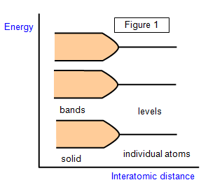
In a solid the atoms
are linked together and the electrons can occupy a whole series of energy levels grouped into
bands (see Figure 1). The difference in energy between levels within the band is very small
compared with the energy gap between the bands. The electrical differences between one type
of solid and another lie in the different arrangements of the bands.
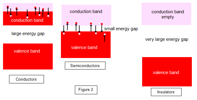
The band structures
of a conductor, semiconductor and insulator are shown in Figure 2.

In the intrinsic semiconductor the valence band is full once more, but the
conduction band is empty at very low temperatures. However, the energy gap between the two
bands is so very small that electrons can jump across it by the addition of thermal energy alone
or even light energy of a suitable wavelength. In other words, heating the specimen or shining a
light on it maybe sufficient to cause electrical conduction. The conductivity increases with
temperature as more and more electrons are liberated. Semiconductors therefore have negative
temperature coefficients of resistance.
For germanium the energy gap is 0.66 eV and
for silicon it is 1.11 eV at 27 oC. When an electron jumps to the conduction band it leaves behind
it a space or hole in the valence band. This hole is effectively positive and since an electron can
jump into it from another part of the valence band it is as if the hole itself was moving!
Conduction can take place either by negative electrons moving within the conduction band or by
positive holes moving within the valence band.

A semiconductor may be thought of as similar
to an almost full multi-storey car park, the cars representing the electrons and the spaces the
holes (no cars are allowed to enter or leave the car park, however, only to drive round within it!).
(Figure 3)
If this idea of holes seems odd to you, think of a pile of
earth and the hole in the road from which it came. Both the pile (electron) and the hole (hole)
have a physical effect on you if you run into them on a bike! Conduction by positive holes is
rather like workmen digging up a road; in a way, they are only moving a hole from one place to
another.
In the insulator the valence band is full once again, but in these substances the energy gap between this and the empty conduction band is very large. It would take a great deal of energy to make an electron jump the gap and to cause the insulator to break down. At very high temperatures or under very large electric fields breakdown will occur, and like semiconductors the greater the temperature the greater the conduction. Insulators, like semiconductors, have negative temperature coefficients of resistance.
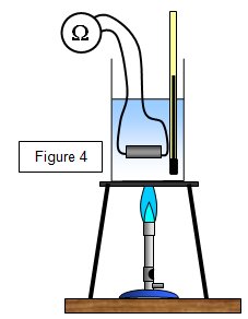
 The thermistor is a semiconductor device whose resistance changes markedly with temperature.
 An extrinsic semiconductor is basically a semiconductor to which a
very small amount of impurity has been added. About one atom per million is replaced by an
impurity atom; this process is called doping.
Doping with an impurity can have quite marked
effects on the electrical properties of the material. The addition of one impurity atom in one
hundred million will increase the conductivity of germanium by twelve times at 300 K. Very
precise doping may be achieved by neutron irradiation.


(b) p-type, by doping with trivalent material such as
aluminium.
The effect of both types of doping is shown in the diagram. With the p-type
each impurity atom has one fewer electron than the silicon atom, while with the n-type they have
one extra electron.
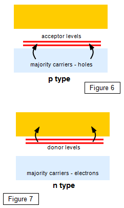
Figures 6 and 7 show how the impurity atoms fit into the energy
level diagram of the solid as a whole. In the p-type material the aluminium levels fall just above
the full valence band of the silicon. These levels are very close to this band and so electrons
can easily jump into them from the valence band. For this reason they are called acceptor
levels. When an electron jumps up to these levels it leaves behind a hole in the valence band; it
is the movement of holes within the valence band that causes the greatest conduction in a p-
type material. In the n-type material the phosphorus energy levels fall just below the empty
conduction band of the silicon, and very close to it. For this reason electrons can very easily
jump from them into the conduction band, and they are therefore called donor levels. In n-type
material conduction takes place mainly due to the movement of these
electrons.